


HI!
First of all i hope that i don,t make any mistake by not folowing the topic :"mSATA on the X201: its possible",but time ago when i google for x200 msata mod i couldnt findit. i find it only with x201 msata mod in search
This mod have 2 parts:
PART 1 adding an msata ssd using the docking connector
It aloww me to boot ,it the bios see it ,but it dindt alow me to set a password or to do secure erase form bios,but if i run a linux distribution,i can make secure erase .I thing the problem is in the fact that i don,t have all the necessary signal to "inform" the bios about the second HDD.I would like to knew from somone that have the docking station,if is posible to set the HDD pasword for secondary HDD.
http://imageshack.us/a/img854/9508/starta.jpg
First of all we need to solder 5 cable to the docking station connector(i have use IDE cable -2 wire for data/ground/2 wire data),and cover it with thin foil..
http://imageshack.us/a/img829/9311/msat ... innote.jpg
Because i use the docking connector,i,ve chose a way to connect the ssd,so in case that i use the docking station,to be easy to remove the SSD.For this purpose,decided to use the expres card slot..In case of "emergency",just open the palmrest,and get out the msata ,without needed to unsolder anything.The msata socket allow the card to be pushed orizontaly,like the expres card.Is a "unortodox" way of using the connector,but it work.
http://imageshack.us/a/img801/5459/msat ... etb.th.jpg
http://imageshack.us/a/img338/4480/msatamodsoketc.jpg
It is also posibly to solder 4 more wire in paralell with the msata connector and put an esata connector.In this way we can have esata or msata...Or it can be more easy to use an old hdd connector with sata_line pin so we can use an simple sata cable (an esata complet socket is hard to fit inside the exprescard so that we can "hide " everything with the door
http://imageshack.us/a/img715/9970/msat ... tdnote.jpg
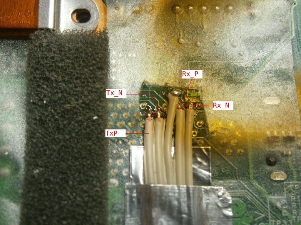
I,ve connected ground i both end of sata cable(docking an msata connector),a suplimentary ground from the board to the msata conector,and 3,3 v from original hdd.In the Msata connector we need to connect pin 39,41 to vcc and 35,37,49 to ground...23-RXP,25-RXN,27&29-gnd,31-TXN ,33-TXP
PART 2 underclocking FSB=800,undervoltage
WIFI ,bluetooth,wwan off display minimum power consumption 4.3w...i still need to make few benchmark but i think that for a X200 (non S) is prety good
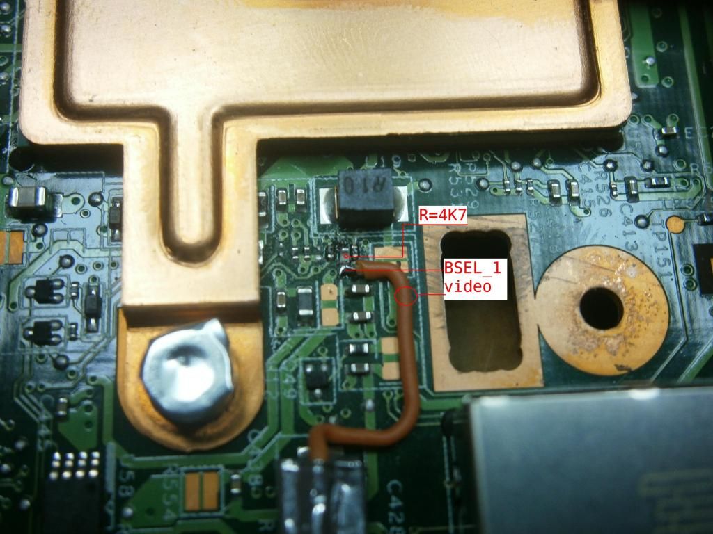
The Cpu send the clock select command to 2CI : video card (for the moment i dont,touch it),and Clk_Generator..Normal for 266 FSB the controls are bsel2,bsel1,bsel0 : 0,0,0...For a FSB of 200 are 0,1,0 so i,ve desconnected the bsel1 from CPU,and connected to a 3,3 volt with a 47k resistor,to give it a 1 level..I,ve used wire because in the futre i wish to use a switch so i could change the FSB,without opening the case.The switch will be in the expres card behind the door..
http://imageshack.us/a/img843/8315/vidm ... rmance.jpg
First will cut the connection betwen CPU and clock_generator (in theory should,nt be any problem if wil connect directily to VCC cpu,but i prefer this way,to be safe).
http://imageshack.us/a/img405/2585/bsel ... nnotea.jpg
We use a wire (orange in my case),to route the input signal of clk_geneartor,to the other side of board,when i,ve made the connection.On the top side of board we can connect a wire (white in my case) to the CPU_out signal (we already cut the trace in the previous phase (in picture it is writed CUT).
http://imageshack.us/a/img715/4012/bsel1cpuout.jpg
from that moment we can use Normal mode :cpuout connected with clk_gen_in,or underclocked cpu_out not connected and clk_gen connected WITH a 47K resistor to 3,3v... (in the final image of the expres card with msata you can see in the left corner the provisional board that i,ve used for making the conections
For underclocking we ned to connect VID4 to 1 level .in this way for voltage betwen 0 ant 0.9v and 1.1 to 1.4 volt everything is ok.the "theoretical" voltage that are controled from cpu are identicaly with the real one.For tension betwen 0.9 and 1,1 v,the real tension are 0,2 volt less .P8600 in start mode need 1,2 volt =>ok,0.875v minim=>ok and 1,1375 volt that is also ok .(facke voltage are only betven 0.9 and 1.1volt).Ive used CPUgenie.and underclock tha CPU to 0.7125v-selected 0.9125 and the real tension are 0.7125.
With this modification FSB are 200 minim 600Mhz -0.7125v maxim 1800Mhz -0.850volt
We need to cut trace to VID4 and connect to VCC so we can have level 1
http://imageshack.us/a/img27/8366/vid4modfinala.jpg
This is my first post so if i made any mistake ,i ask you apologies (especialy for the way of expresing myself,english is not my "natural talent".Ive tried to put big image (<1M) where was necesary.
I was inspired from the chinese page about adding msata to x201,page that i,ve discovered thanks to OP of "mSATA on the X201: its possible",surfboy
One interesting thing about docking connector: when i was try to connect directly to the chipset,(because it was more close to exprescard slot)it doesn,t work ,I thing that are some kind of pcb inductance in board betwen the chipset and connector
Take a look at our
ThinkPads.com HOME PAGE
For those who might want to contribute to the blog, start here: Editors Alley Topic
Then contact Bill with a Private Message
ThinkPads.com HOME PAGE
For those who might want to contribute to the blog, start here: Editors Alley Topic
Then contact Bill with a Private Message
X200 msata mod, underclock mod WARNING PICTURES
X200 msata mod, underclock mod WARNING PICTURES
First_Love: Thinkpad 600
Actual: TP T61,T8100,3G ram,win_XP ,fujitsu_FDE,docking // X200,m-sata_mod,P8600,4G ram,LED,Intel 5100 ,WWAN mc8755 ,GPS GTM378,PM810_FDE_ssd // X41_tabblet 1,6 ghz,sata_mod samsung_pm830,
over time: X30,31 T30,40,41 X60,61 60_Tabblet
Actual: TP T61,T8100,3G ram,win_XP ,fujitsu_FDE,docking // X200,m-sata_mod,P8600,4G ram,LED,Intel 5100 ,WWAN mc8755 ,GPS GTM378,PM810_FDE_ssd // X41_tabblet 1,6 ghz,sata_mod samsung_pm830,
over time: X30,31 T30,40,41 X60,61 60_Tabblet
-
bretahrnek
- Freshman Member
- Posts: 72
- Joined: Sun Jul 08, 2012 9:59 am
- Location: United Kingdom, Sheffield
Re: X200 msata mod, underclock mod WARNING PICTURES
Amazing job,
do You think that can you upload more pics , in higher resolution please?
regards Brett
do You think that can you upload more pics , in higher resolution please?
regards Brett
mainly in use : X201.i5.8GB.**AFFS**.120GBVertex4.Intel6300.GOBI2000.NMD.Ultrabase.w7Pro64
other : T410s.i5.8GB.120GBVertex4.Intel6300.GOBI2000.NMD.w7Pro64
others : X60 | T43p.UXGA.sata | 600e | X300 | T61p
ex : Edge.11 | T60.UXGA.T9500
other : T410s.i5.8GB.120GBVertex4.Intel6300.GOBI2000.NMD.w7Pro64
others : X60 | T43p.UXGA.sata | 600e | X300 | T61p
ex : Edge.11 | T60.UXGA.T9500
Re: X200 msata mod, underclock mod WARNING PICTURES
Great Job !!!
+1 : Please provide links to high resolution pic
regards,
+1 : Please provide links to high resolution pic
regards,
ex: A31-2652-D5G with 1GB Ram
Re: X200 msata mod, underclock mod WARNING PICTURES
HI!
I,ve uploaded new photos,with more resolution (aproximativly 1,3M).I also add the video chipset clok select mod.Now we have 2 wire (CLK_gen IN + Video IN) conected thighether on the bottom of the board.Actualy ,ive passed a wire from vidoe chipset to the clock_gen in ,cut the trace betwen clok gen and CPU_out,and made a switch with 2 position : Normal SEL+CPU_out,and Low_power SEL+3v with a 47k resistor..FOr the moment I didnt have the time to test a long time the modification of the video clock..Just can say that it worck and the meory time before was 7-7-7-20 and now are 6-6-6-16..I hope that someone can tell me if this mean something or no,I knew that this are memory timing..I will put more pictures(Msata connector in the expres card,etc) and benchmark in more day,For moment my time is limited because a scary thing is hunting me : Mathematics exams....

dockimg conector SATA signals:
http://i1297.photobucket.com/albums/ag2 ... 0db662.jpg
CLK_GEN_input_bootom_side (originaly where i,ve made the solders it was a smal 2k2 resistor,but ,ive elminated it)
http://i1297.photobucket.com/albums/ag2 ... 1b2713.jpg
http://i1297.photobucket.com/albums/ag2 ... c0a799.jpg
Video_chipse clk BSEL.Here where i put the resistor,it was a small 1k1 resistor ,conected to the trace from CPU with a plated hole.I,ve eleminated his resistor,and with a fine drill cut the metalization.Is easy to find because the original resistor is smaller then mine .Also woul be better to just cut the trace instead of driling the plated hole.I DIDNT DRILL FROM TOP TO BOTTOM,only a litlle on the surface.
http://i1297.photobucket.com/albums/ag2 ... 81fead.jpg
I,ve used the small plated hole from top side to get original CPU clock
http://i1297.photobucket.com/albums/ag2 ... 6701f1.jpg
http://i1297.photobucket.com/albums/ag2 ... 5b1b8e.jpg
If someone wish,i can give it the biger photos (3MB),that are BMP,but i dont,think will be a bigger diference.Being new in the forum i don,t knew how is better to keep puting replys,or editing the original post so can be a "complet" manual..Mybe someone is willig to corect my spelling...
link so that can download full size image aprox 1,5 Mb each
http://s1297.beta.photobucket.com/user/totenko/profile/
I,ve uploaded new photos,with more resolution (aproximativly 1,3M).I also add the video chipset clok select mod.Now we have 2 wire (CLK_gen IN + Video IN) conected thighether on the bottom of the board.Actualy ,ive passed a wire from vidoe chipset to the clock_gen in ,cut the trace betwen clok gen and CPU_out,and made a switch with 2 position : Normal SEL+CPU_out,and Low_power SEL+3v with a 47k resistor..FOr the moment I didnt have the time to test a long time the modification of the video clock..Just can say that it worck and the meory time before was 7-7-7-20 and now are 6-6-6-16..I hope that someone can tell me if this mean something or no,I knew that this are memory timing..I will put more pictures(Msata connector in the expres card,etc) and benchmark in more day,For moment my time is limited because a scary thing is hunting me : Mathematics exams....
dockimg conector SATA signals:
http://i1297.photobucket.com/albums/ag2 ... 0db662.jpg
CLK_GEN_input_bootom_side (originaly where i,ve made the solders it was a smal 2k2 resistor,but ,ive elminated it)
http://i1297.photobucket.com/albums/ag2 ... 1b2713.jpg
http://i1297.photobucket.com/albums/ag2 ... c0a799.jpg
Video_chipse clk BSEL.Here where i put the resistor,it was a small 1k1 resistor ,conected to the trace from CPU with a plated hole.I,ve eleminated his resistor,and with a fine drill cut the metalization.Is easy to find because the original resistor is smaller then mine .Also woul be better to just cut the trace instead of driling the plated hole.I DIDNT DRILL FROM TOP TO BOTTOM,only a litlle on the surface.
http://i1297.photobucket.com/albums/ag2 ... 81fead.jpg
I,ve used the small plated hole from top side to get original CPU clock
http://i1297.photobucket.com/albums/ag2 ... 6701f1.jpg
http://i1297.photobucket.com/albums/ag2 ... 5b1b8e.jpg
If someone wish,i can give it the biger photos (3MB),that are BMP,but i dont,think will be a bigger diference.Being new in the forum i don,t knew how is better to keep puting replys,or editing the original post so can be a "complet" manual..Mybe someone is willig to corect my spelling...
link so that can download full size image aprox 1,5 Mb each
http://s1297.beta.photobucket.com/user/totenko/profile/
First_Love: Thinkpad 600
Actual: TP T61,T8100,3G ram,win_XP ,fujitsu_FDE,docking // X200,m-sata_mod,P8600,4G ram,LED,Intel 5100 ,WWAN mc8755 ,GPS GTM378,PM810_FDE_ssd // X41_tabblet 1,6 ghz,sata_mod samsung_pm830,
over time: X30,31 T30,40,41 X60,61 60_Tabblet
Actual: TP T61,T8100,3G ram,win_XP ,fujitsu_FDE,docking // X200,m-sata_mod,P8600,4G ram,LED,Intel 5100 ,WWAN mc8755 ,GPS GTM378,PM810_FDE_ssd // X41_tabblet 1,6 ghz,sata_mod samsung_pm830,
over time: X30,31 T30,40,41 X60,61 60_Tabblet

Re: X200 msata mod, underclock mod WARNING PICTURES
Wow, I'm definitely impressed.
I don't feel qualified to even attempt this on my machine, but a great read. Keep up the modding!
I don't feel qualified to even attempt this on my machine, but a great read. Keep up the modding!
Current: 13 (1st gen) - i3-6200U - 8GB - 128GB - FHD (Got it for $250  )
)
Previous: X60s | X200s | X230 | X240sx | X1 Carbon (3rd) | TPY260 | X1 Yoga (1st)
Projects: 560 | 600E | T21
Previous: X60s | X200s | X230 | X240sx | X1 Carbon (3rd) | TPY260 | X1 Yoga (1st)
Projects: 560 | 600E | T21
Re: X200 msata mod, underclock mod WARNING PICTURES
hi,
gr8 work..was thinking about if it would be possible to make all process easier..so..
According to that pict:
msata and minipcie have first 6 ports similar - if am wrong please correct me..
so buying that part: http://www.alibaba.com/product-gs/46486 ... _Card.html
disconnect the wide part of extender and soldering sata ports A+,A-,B+,B- to sata-docking station ports should make a job
if am wrong please correct me
ex: A31-2652-D5G with 1GB Ram
Re: X200 msata mod, underclock mod WARNING PICTURES
Hola
Buscando información sobre cómo añadir un disco msata a un thinkpad x201 he llegado hasta aquí, pero no me queda del todo claro por lo que me permito haceros unas preguntas.
¿Hay que parchear la BIOS? Si es así, dónde puedo bajarla
¿Funcionaria el nuevo disco msata simultáneamente con el antiguo?
¿Podríais volver a subir las fotos de imageshack?
Gracias.
-
RealBlackStuff
- Admin Emeritus

- Posts: 24554
- Joined: Mon Sep 18, 2006 5:17 am
- Location: Loch Garman, Éire
Re: X200 msata mod, underclock mod WARNING PICTURES
Welcome to the Forum.
Unfortunately you replied to a thread from more than three years ago.
User totenko has also not been seen on the forum since then, so I doubt he can refresh those imageshack pictures...
But maybe another forum member still has them. Anybody?
Furthermore, this is an English-language only forum (although some of us also know Spanish).
Lovely day for a Guinness! (The Real Black Stuff)
But I actually prefer Murphy's from Cork!
But I actually prefer Murphy's from Cork!
Re: X200 msata mod, underclock mod WARNING PICTURES
I’m sorry, i'll write in English.
Thanks for the answer
Thanks for the answer
Re: X200 msata mod, underclock mod WARNING PICTURES
Guys, I need help.
I've soldered all data and ground cables between mSata Plextor disk and MB and steal voltage from Sata.
After this - nothing. Do i need to do something else? Something to tell MB that second disk is connected?
I've soldered all data and ground cables between mSata Plextor disk and MB and steal voltage from Sata.
After this - nothing. Do i need to do something else? Something to tell MB that second disk is connected?
-
- Similar Topics
- Replies
- Views
- Last post
-
-
WTB :LED INVERTER MOD + LVDS CABLE MOD FOR T61p
by pyrrhus » Thu Apr 10, 2025 2:12 pm » in Marketplace - Forum Members only - 0 Replies
- 1668 Views
-
Last post by pyrrhus
Thu Apr 10, 2025 2:12 pm
-
-
-
What is a recommended usage for the mSATA slot?
by lmm0312tpforum » Fri Apr 04, 2025 8:19 am » in ThinkPad X200/X201/X220 and X300/X301 Series - 3 Replies
- 2135 Views
-
Last post by axur-delmeria
Fri Apr 04, 2025 8:29 pm
-
-
-
W530 throughput comparison mSATA vs ExpressCard to NVMe adaptor?
by ac427 » Sun Jul 20, 2025 1:52 pm » in ThinkPad W530/W540/W541/W550 Series - 9 Replies
- 5456 Views
-
Last post by ogopogo
Sun Sep 14, 2025 5:50 pm
-
-
-
Thinkpad T41p mSATA to IDE route
by thinkpadt41p » Fri Sep 12, 2025 12:01 pm » in ThinkPad T40/T41/T42/T43 Series - 4 Replies
- 1408 Views
-
Last post by Glaurung-quena
Mon Sep 15, 2025 1:52 am
-
Who is online
Users browsing this forum: No registered users and 9 guests